


 Flexible Thinking: PCB Designers Still Wanted
 Connect the Dots: Five Best Practices for Designing Flex and Rigid-flex PCBs
 Tim’s Takeaways: Human Ingenuity and the Rigid-flex PCB
Toward Imperceptible Electronics That You Cannot See or Feel
January 11, 2021 | Osaka UniversityEstimated reading time: 1 minute
Transparent electronics—such as head-up displays that allow pilots to read flight data while keeping their eyes ahead of them—improve safety and allow users to access data while in transit. For healthcare applications, the electronics need to not only be cheap and straightforward to fabricate, but also sufficiently flexible to conform to skin. Silver nanowire networks meet these criteria. However, current methods of development create random nanowire alignment that's insufficient for advanced applications.
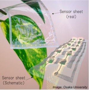
In an upcoming study in Advanced Intelligent Systems, researchers from Osaka University have used high-resolution printing to fabricate centimeter-scale cross-aligned silver nanowire arrays, with reproducible feature sizes from 20 to 250 micrometers. As a proof-of-concept for functionality, they used their arrays to detect electrophysiological signals from plants.
The researchers first created a patterned polymer surface to define the subsequent nanowire feature size. Using a glass rod to sweep silver nanowires across the pattern led to either parallel or cross-aligned nanowire networks, depending on the direction of the sweep. Nanowire cross-alignment, alignment within the pattern, and electro-optical properties were impressive.
"The sheet resistance of patterns less than 100 micrometers ranged from 25 to 170 ohms per square, and the visible light transmittance at 550 nanometers was 96% to 99%," says Teppei Araki, co-senior author. "These values are well-suited for transparent electronics."
The researchers showed off the utility of their technology by monitoring the electric potential of Brazilian waterweed leaves. Because the nanowire arrays are transparent, the researchers were able to keep the leaf under visual observation while acquiring data over long periods of time. A 2- to 3-micrometer-thick device conformed to the surface of a leaf without causing damage.
"Our microelectrodes-based organic field-effect transistors exhibited excellent multi-fuctionality," says Tsuyoshi Sekitani, co-senior author. "For example, transparency of 90%, the on–off ratio was ~106, and the leakage current remained stable upon bending at a radius of 8 millimeters."
Transparent electronics is an emerging technology. It must be simple and inexpensive to mass-produce for biomedicine, civil engineering, agriculture, and other applications that require underlying visual observation. The advance described here is an important step in that direction. The Osaka University researchers plan on making further technical improvements, such as incorporating graphene onto the nanowire’s surface. This will improve the uniformity of the microelectrodes' sheet resistance. Ultimately, the researchers' technology will help minimize the raw material input of electronics, and exceed the functionality of conventional non-transparent electronics.
Read the original article, here.
Share on:


Suggested Items
Book Excerpt: The Printed Circuit Assembler’s Guide to... Factory Analytics
04/24/2024 | I-Connect007 Editorial TeamIn our fast-changing, deeply competitive, and margin-tight industry, factory analytics can be the key to unlocking untapped improvements to guarantee a thriving business. On top of that, electronics manufacturers are facing a tremendous burden to do more with less. If you don't already have a copy of this book, what follows is an excerpt from the introduction chapter of 'The Printed Circuit Assembler’s Guide to... Factory Analytics: Unlocking Efficiency Through Data Insights' to whet your appetite.
Listen Up! The Intricacies of PCB Drilling Detailed in New Podcast Episode
04/25/2024 | I-Connect007In episode 5 of the podcast series, On the Line With: Designing for Reality, Nolan Johnson and Matt Stevenson continue down the manufacturing process, this time focusing on the post-lamination drilling process for PCBs. Matt and Nolan delve into the intricacies of the PCB drilling process, highlighting the importance of hole quality, drill parameters, and design optimization to ensure smooth manufacturing. The conversation covers topics such as drill bit sizes, aspect ratios, vias, challenges in drilling, and ways to enhance efficiency in the drilling department.
Elevating PCB Design Engineering With IPC Programs
04/24/2024 | Cory Blaylock, IPCIn a monumental stride for the electronics manufacturing industry, IPC has successfully championed the recognition of the PCB Design Engineer as an official occupation by the U.S. Department of Labor (DOL). This pivotal achievement not only underscores the critical role of PCB design engineers within the technology landscape, but also marks the beginning of a transformative journey toward nurturing a robust, skilled workforce ready to propel our industry into the future.
Winner of The Science Show Rakett 69 Receives Incap Scholarship
04/24/2024 | IncapThe winner of the Rakett 69 science show, Andri Türkson, who stood out as an electronics enthusiast, received a scholarship from Incap Estonia, along with an internship opportunity in Saaremaa.
Alternative Manufacturing Inc. Awarded QML Requalification to IPC J-STD-001 and IPC-A-610
04/24/2024 | IPCIPC's Validation Services Program has awarded an IPC J-STD-001 and IPC-A-610 Qualified Manufacturers Listing (QML) requalification to Alternative Manufacturing Inc (AMI).