


 Flexible Thinking: PCB Designers Still Wanted
 Connect the Dots: Five Best Practices for Designing Flex and Rigid-flex PCBs
 Tim’s Takeaways: Human Ingenuity and the Rigid-flex PCB
AT&S Wins Awards for Sustainable and Environmentally Friendly Production
October 18, 2019 | AT&SEstimated reading time: 2 minutes
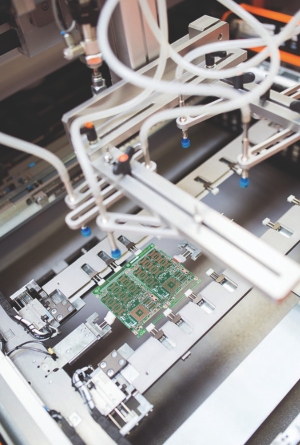
With the presentation of two prestigious awards to the AT&S plants in Shanghai, China, and Nanjangud, India, AT&S was able to demonstrate that the sustainable, efficient and resource-saving production of high-end printed circuit boards has long been a reality for the company.
The AT&S plant in Shanghai, the world's largest production site for HDI printed circuit boards, has been awarded the “National Green Plant Certificate.” This certificate is a key element of the Chinese “Green Manufacturing System” introduced in 2016, which aims at speeding up industrial development in China while maintaining high environmental standards. The seal, which has been awarded to just a handful of China's industrial plants so far, is awarded to outstanding companies that have demonstrated a clear commitment to sustainability in their respective industries and use state-of-the-art technologies and environmentally friendly practices in their production facilities. The innovative water recycling system at the Shanghai site, optimized process management and the implementation of various projects to increase energy efficiency and effectiveness at the AT&S plant were some of the key factors in meeting the necessary certification standards.
AT&S India Receives ELCINA Award
At almost the same time, AT&S India received the ELCINA Award for Excellence in PCB Manufacturing for its Nanjangud production site near the Indian high-tech centre of Bangalore. The prize is awarded annually by the Electronic Industries Association of India (ELCINA) in recognition of outstanding achievements in printed circuit board manufacturing. The ELCINA Award is presented on the basis of strict criteria such as technology upgrades, environmental protection, sustainable growth rate and product complexity and is highly regarded in the field of electronics manufacturing in India.
“I am delighted that our efforts in the area of environmentally friendly and at the same time economically efficient, sustainable production of high-end printed circuit boards are being acknowledged,” says AT&S CEO Andreas Gerstenmayer. “In the long term, our goal is to become the benchmark for the industry as a whole and to live up to our environmental, economic and social responsibilities as the world's leading supplier of high-end printed circuit board solutions. Being successful as a company in the long term requires that economic success and ecological responsibility are not at odds.”
AT&S Austria Technologie & Systemtechnik AG—First choice for Advanced Applications
AT&S is the European market leader and one of the globally leading manufacturers of high-value printed circuit boards and IC substrates. AT&S industrialises leading-edge technologies for its core business segments Mobile Devices, Automotive, Industrial, Medical and Advanced Packaging. AT&S has a global presence, with production facilities in Austria (Leoben and Fehring) and plants in India (Nanjangud), China (Shanghai, Chongqing) and Korea (Ansan, near Seoul). The company employed an average of about 10,000 people in the financial year 2017/18. For more information: www.ats.net
Share on:


Suggested Items
Real Time with… IPC APEX EXPO 2024: Tools, Training, and Trends in Manufacturing Engineering
04/25/2024 | Real Time with...IPC APEX EXPOGuest Editor Kelly Dack and Product Specialist Erik Bateham of Polar Instruments discuss Polar's latest technology, including their role in aiding manufacturing engineers. They highlight the advanced capabilities of Polar's tools and the critical role of signal integrity analysis, as well as the importance of accurate modeling in board manufacturing. Polar's unique training approach and demonstration contact details are also explored.
TTM Celebrates the Grand Opening of Its First Manufacturing Facility in Penang
04/25/2024 | TTM Technologies, Inc.TTM Technologies, Inc., a leading global manufacturer of technology solutions including mission systems, radio frequency (RF) components and RF microwave/microelectronic assemblies, and quick-turn and technologically advanced printed circuit boards (PCBs), officially opened its first manufacturing plant in Penang, Malaysia with an investment of USD200 million (approximately RM958 million).
Listen Up! The Intricacies of PCB Drilling Detailed in New Podcast Episode
04/25/2024 | I-Connect007In episode 5 of the podcast series, On the Line With: Designing for Reality, Nolan Johnson and Matt Stevenson continue down the manufacturing process, this time focusing on the post-lamination drilling process for PCBs. Matt and Nolan delve into the intricacies of the PCB drilling process, highlighting the importance of hole quality, drill parameters, and design optimization to ensure smooth manufacturing. The conversation covers topics such as drill bit sizes, aspect ratios, vias, challenges in drilling, and ways to enhance efficiency in the drilling department.
Elevating PCB Design Engineering With IPC Programs
04/24/2024 | Cory Blaylock, IPCIn a monumental stride for the electronics manufacturing industry, IPC has successfully championed the recognition of the PCB Design Engineer as an official occupation by the U.S. Department of Labor (DOL). This pivotal achievement not only underscores the critical role of PCB design engineers within the technology landscape, but also marks the beginning of a transformative journey toward nurturing a robust, skilled workforce ready to propel our industry into the future.
Fujitsu, METRON Collaborate to Drive ESG Success
04/24/2024 | JCN NewswireFujitsu Limited and METRON SAS, a French cleantech company specializing in energy management solutions for industrial decarbonization, today announced a strategic initiative to contribute to the realization of carbon neutrality in the manufacturing industry.