


 Flexible Thinking: PCB Designers Still Wanted
 Connect the Dots: Five Best Practices for Designing Flex and Rigid-flex PCBs
 Tim’s Takeaways: Human Ingenuity and the Rigid-flex PCB
A Flexible Future
February 20, 2019 | UNSW SydneyEstimated reading time: 2 minutes
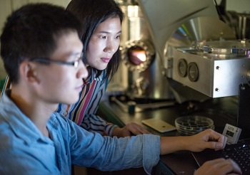
Thin, flexible panels that will revolutionise how we use solar energy are on the drawing board at UNSW. Imagine a future in which thin, flexible solar panels cover the surfaces of cars and buildings, powering their activities.
Xiaojing Hao, associate professor and Scientia fellow in the School of Photovoltaic and Renewable Energy Engineering, and her team, are building such cells made of kesterite photovoltaics.
Containing copper, zinc, tin and sulphur, they are cheaper to make and more environmentally friendly than other thin-film varieties on the market, some of which contain toxic materials, such as cadmium, or rare elements, such as indium and tellurium.
There are significant industrial applications for flexible, thin photovoltaic cells. But a key challenge has been their limited capacity to generate energy with a comparable efficiency and cost to that of conventional silicon solar panels.
In 2017, A/Prof Hao’s team built a kesterite photovoltaic cell that attained 11% efficiency. This set a world record—a fourth for the team—and was the first time that the 10% efficiency threshold was broken for this type of cell. This work was published in the Nature Energy journal in 2018.
“For each efficiency change, we need a step-change technology to make it happen,” says A/Prof Hao. She hopes to improve the efficiency of kesterite photovoltaic cells to close to 20% in the next five years.
To do this, her team needs to work out how to prevent the common defects in the lattice of the kesterite material. The reasons for these defects are not yet well understood. However, once corrected, the electrical quality of the material—the main barrier to efficiency—will improve.
Exciting findings from 2018 point to some new directions to control the defects and improve the performance of kesterite cells. The plan is to apply for Australian Research Council funding to delve deeper and publish some of these results in 2019.
Dr Xiaojing Hao of UNSW's Australian Centre for Advanced Photovoltaics holding the new CZTS solar cells.
In 2017, A/Prof Hao was one of 18 young scientists selected from more than 1000 applicants to take up one of UNSW’s inaugural Scientia fellowships. Last year, she won two prestigious prizes: the $5000 Premier’s Prize for Energy Innovation from the state of New South Wales and the $3000 UNSW Engineering Faculty Dean’s Award for Excellence in Research. A/Prof Hao’s enthusiasm for discovery is given free rein at UNSW.
“I love to explore the unknowns and deal with challenges. Achieving research progress, particularly through challenging work, brings me deep fulfilment.”
Share on:


Suggested Items
Designer’s Notebook: What Designers Need to Know About Manufacturing, Part 2
04/24/2024 | Vern Solberg -- Column: Designer's NotebookThe printed circuit board (PCB) is the primary base element for providing the interconnect platform for mounting and electrically joining electronic components. When assessing PCB design complexity, first consider the component area and board area ratio. If the surface area for the component interface is restricted, it may justify adopting multilayer or multilayer sequential buildup (SBU) PCB fabrication to enable a more efficient sub-surface circuit interconnect.
Insulectro’s 'Storekeepers' Extend Their Welcome to Technology Village at IPC APEX EXPO
04/03/2024 | InsulectroInsulectro, the largest distributor of materials for use in the manufacture of PCBs and printed electronics, welcomes attendees to its TECHNOLOGY VILLAGE during this year’s IPC APEX EXPO at the Anaheim Convention Center, April 9-11, 2024.
ENNOVI Introduces a New Flexible Circuit Production Process for Low Voltage Connectivity in EV Battery Cell Contacting Systems
04/03/2024 | PRNewswireENNOVI, a mobility electrification solutions partner, introduces a more advanced and sustainable way of producing flexible circuits for low voltage signals in electric vehicle (EV) battery cell contacting systems.
Heavy Copper PCBs: Bridging the Gap Between Design and Fabrication, Part 1
04/01/2024 | Yash Sutariya, Saturn Electronics ServicesThey call me Sparky. This is due to my talent for getting shocked by a variety of voltages and because I cannot seem to keep my hands out of power control cabinets. While I do not have the time to throw the knife switch to the off position, that doesn’t stop me from sticking screwdrivers into the fuse boxes. In all honesty, I’m lucky to be alive. Fortunately, I also have a talent for building high-voltage heavy copper circuit boards. Since this is where I spend most of my time, I can guide you through some potential design for manufacturability (DFM) hazards you may encounter with heavy copper design.
Trouble in Your Tank: Supporting IC Substrates and Advanced Packaging, Part 5
03/19/2024 | Michael Carano -- Column: Trouble in Your TankDirect metallization systems based on conductive graphite or carbon dispersion are quickly gaining acceptance worldwide. Indeed, the environmental and productivity gains one can achieve with these processes are outstanding. In today’s highly competitive and litigious environment, direct metallization reduces costs associated with compliance, waste treatment, and legal issues related to chemical exposure. What makes these processes leaders in the direct metallization space?