


 Flexible Thinking: PCB Designers Still Wanted
 Connect the Dots: Five Best Practices for Designing Flex and Rigid-flex PCBs
 Tim’s Takeaways: Human Ingenuity and the Rigid-flex PCB
AT&S Receives HELLA Innovation Award
July 9, 2019 | AT&SEstimated reading time: 1 minute
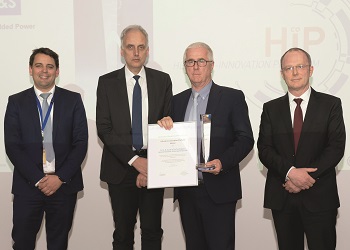
HELLA, an internationally operating German automotive supplier, has honoured particularly innovative suppliers. Numerous companies from various industries took part in the new “HELLA Co-Innovation Platform” (HIP) competition and presented their innovation proposals to a jury consisting of members of the Electronics executive board and further experts. Following an extensive evaluation, AT&S reached the final with its “PCB Embedded Power” submission, along with two other suppliers. In the innovative concept by AT&S, power components such as MOSFETs are embedded directly in the PCB. A considerable size reduction in a relevant product was demonstrated to HELLA.
“For AT&S, this award from HELLA is an important recognition that we are an innovation driver and expert partner,” said a delighted Heinz Moitzi, AT&S COO. “The award is another step on our way to becoming a provider of comprehensive and powerful interconnect solutions that go far beyond just the circuit board.”
The aim of the HIP competition is to involve particularly innovative suppliers in the early phases of product development and thus jointly advance the development of new, forward-looking technologies. AT&S has now been honoured as a particularly innovative supplier to HELLA at an awards ceremony at the company’s headquarters in Lippstadt. Innovative strength, cost-effectiveness and cooperation potential with regard to HELLA’s product and development portfolio were the winning criteria.
AT&S PCB Embedded Power
Based on the AT&S ECP (embedded components packaging) technology, integrated active and passive components are integrated into PCBs for low-power designs and are used in volume production meeting high-quality requirements. Accordingly, the implementation of power semiconductors like MOSFETs directly into the circuit board (PCB Embedded Power) is a very promising approach for meeting the increasing needs of electromobility and challenging industrial applications. Efficient power packaging solutions and power modules can be implemented in this way. Compared to conventional SMT technology, a space reduction for the power module of 50% can be realized, significantly increasing the power density. In addition, the innovative power packaging technology offers very good results in terms of switching behaviour, heat removal and power cycling robustness.
Share on:


Suggested Items
Samsung Electronics Begins Industry’s First Mass Production of 9th-Gen V-NAND
04/29/2024 | Samsung ElectronicsSamsung Electronics, the world leader in advanced memory technology, today announced that it has begun mass production for its one-terabit (Tb) triple-level cell (TLC) 9th-generation vertical NAND (V-NAND), solidifying its leadership in the NAND flash market.
TSMC Celebrates 30th North America Technology Symposium
04/29/2024 | TSMCTSMC unveiled its newest semiconductor process, advanced packaging, and 3D IC technologies for powering the next generation of AI innovations with silicon leadership at the Company’s 2024 North America Technology Symposium.
QinetiQ Achieves UK’s First Jet-to-Jet Teaming Between Aircraft and Autonomous Drone
04/29/2024 | QinetiQQinetiQ has successfully trialled the UK’s first Crewed-Uncrewed-Teaming demonstration between a crewed aircraft and an autonomous jet drone.
Warm Windows and Streamlined Skin Patches – IDTechEx Explores Flexible and Printed Electronics
04/26/2024 | IDTechExFlexible and printed electronics can be integrated into cars and homes to create modern aesthetics that are beneficial and easy to use. From luminous car controls to food labels that communicate the quality of food, the uses of this technology are endless and can upgrade many areas of everyday life.
iNEMI Packaging Tech Topic Series: Role of EDA in Advanced Semiconductor Packaging
04/26/2024 | iNEMIAdvanced semiconductor packaging with heterogenous integration has made on-package integration of multiple chips a crucial part of finding alternatives to transistor scaling. Historically, EDA tools for front-end and back-end design have evolved separately; however, design complexity and the increased number of die-to-die or die-to-substrate interconnections has led to the need for EDA tools that can support integration of overall design planning, implementation, and system analysis in a single cockpit.