


 Flexible Thinking: PCB Designers Still Wanted
 Connect the Dots: Five Best Practices for Designing Flex and Rigid-flex PCBs
 Tim’s Takeaways: Human Ingenuity and the Rigid-flex PCB
Atotech Launches Next Revolution in Electroless Copper for Advanced FPCB
September 3, 2018 | AtotechEstimated reading time: 2 minutes
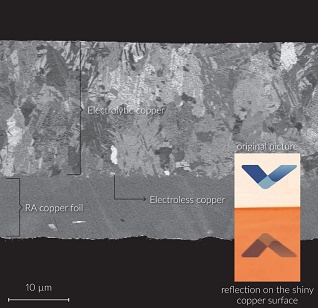
Atotech introduces a new horizontal electroless copper process specifically developed to ensure a blister-free electroless copper deposition and shiny surface appearance after electrolytic copper plating. The new process, Printoganth RA, is compatible with electro-deposited copper (ED), rolled and annealed (RA) as well as “super-flexible RA” (HA) copper foils and best suited to meet OEM requirements for mobile applications.
Image Caption: Printoganth RA – Shiny surface appearance after electrolytic copper plating moderated growth of copper crystals.
RA copper foils are most commonly used for the metallization of next generation flexible substrates. Their special crystal structure, particularly for the “super flexible” HA copper foils, however, requires sophisticated plating solutions in order to achieve the desired surface morphology. One major challenge is the surface appearance after the electrolytic copper plating step. The surface has to have a certain shiny appearance, in order to enable an even etching during structuring and to ensure a reliable automated optical inspection (AOI). In order to overcome this challenge and offer a technically sound solution the Atotech team developed the new Printoganth RA process that complies with different materials when plating advanced flexible and flex-rigid PCBs.
Phenomenal Throwing Power Meets Excellent Coverage with Good Adhesion
Printoganth RA features an excellent coverage on all relevant base materials, including FR4, PI and PI adhesives. A phenomenal throwing power of more than 70% into blind micro vias (BMV) enables good coverage and thicker electroless copper deposits, also at critical spots such as the BMV corners or on exposed adhesive layers within vias. Due to its favorable internal stress characteristics, Printoganth RA allows for an excellent and blister free adhesion of the electroless deposited copper layer even on smooth substrates like PI.
Customer Verification
“Extensive tests at customer sites have confirmed the outstanding performance of Printoganth RA,” states Lars-Eric Pribyl, global product manager for desmear and metallization at Atotech Group. “Already today, two leading manufacturers of FPCBs for next generation smartphones are currently using the Atotech process, which is favored by leading smartphone OEMs. It is the combination of higher process safety thanks to higher throwing power and higher yield rates due to the shiny surface after electroplating that convinced them.”
About Atotech
Atotech is one of the world’s leading manufacturers of specialty chemicals and equipment for the printed circuit board, IC-substrate and semiconductor industries, as well as for the decorative and functional surface finishing industries. Atotech has annual sales of USD1.2 billion (2017). The company is fully committed to sustainability – we develop technologies to minimize waste and to reduce environmental impact. Atotech has its headquarters in Berlin, Germany, and employs about 4,000 people in over 40 countries. For more information, click here.
Share on:


Suggested Items
The Chemical Connection: Reducing Etch System Water Usage, Part 2
05/02/2024 | Don Ball -- Column: The Chemical ConnectionIn my last column, I reviewed some relatively simple ways to reduce water usage in existing etch systems: cutting down cooling coil water flow, adding chillers to replace plant water for cooling, lowering flow rate nozzles for rinses, etc. This month, I’ll continue with more ways to control water usage in your etcher. Most of these are not easily retrofittable to existing equipment but should be given serious consideration when new equipment is contemplated. With the right combination of add-ons, it is possible to bring the amount of water used in an etch system to almost zero.
Designer’s Notebook: What Designers Need to Know About Manufacturing, Part 2
04/24/2024 | Vern Solberg -- Column: Designer's NotebookThe printed circuit board (PCB) is the primary base element for providing the interconnect platform for mounting and electrically joining electronic components. When assessing PCB design complexity, first consider the component area and board area ratio. If the surface area for the component interface is restricted, it may justify adopting multilayer or multilayer sequential buildup (SBU) PCB fabrication to enable a more efficient sub-surface circuit interconnect.
Insulectro’s 'Storekeepers' Extend Their Welcome to Technology Village at IPC APEX EXPO
04/03/2024 | InsulectroInsulectro, the largest distributor of materials for use in the manufacture of PCBs and printed electronics, welcomes attendees to its TECHNOLOGY VILLAGE during this year’s IPC APEX EXPO at the Anaheim Convention Center, April 9-11, 2024.
ENNOVI Introduces a New Flexible Circuit Production Process for Low Voltage Connectivity in EV Battery Cell Contacting Systems
04/03/2024 | PRNewswireENNOVI, a mobility electrification solutions partner, introduces a more advanced and sustainable way of producing flexible circuits for low voltage signals in electric vehicle (EV) battery cell contacting systems.
Heavy Copper PCBs: Bridging the Gap Between Design and Fabrication, Part 1
04/01/2024 | Yash Sutariya, Saturn Electronics ServicesThey call me Sparky. This is due to my talent for getting shocked by a variety of voltages and because I cannot seem to keep my hands out of power control cabinets. While I do not have the time to throw the knife switch to the off position, that doesn’t stop me from sticking screwdrivers into the fuse boxes. In all honesty, I’m lucky to be alive. Fortunately, I also have a talent for building high-voltage heavy copper circuit boards. Since this is where I spend most of my time, I can guide you through some potential design for manufacturability (DFM) hazards you may encounter with heavy copper design.