


 Flexible Thinking: PCB Designers Still Wanted
 Connect the Dots: Five Best Practices for Designing Flex and Rigid-flex PCBs
 Tim’s Takeaways: Human Ingenuity and the Rigid-flex PCB
AT&S Offers Interconnection Tech for Next-Generation 5G Mobile Communications
June 19, 2018 | AT&SEstimated reading time: 2 minutes
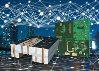
Significantly higher data rates and volumes together with high power densities are resulting in rising requirements for interconnection technologies, too. The new 5G mobile communications generation is undoubtedly an overarching and defining trend here, with applications ranging from infrastructure (base stations) to terminal devices (mobile phones), as well as real-time automation scenarios. AT&S is supporting the current roll-out of the 5G mobile communications generation with high frequency (HF) optimized interconnect solutions and will continue to offer corresponding solutions as the new standard develops.
The launch of the 5G mobile communications generation has far-reaching consequences on the product and system level in terms of miniaturization, functional integration, electromagnetic compatibility (EMC), signal integrity, modularity, safety, security, etc. AT&S therefore analyzed customer requirements and implications for the PCB, substrate and packaging, then initiated and implemented appropriate developments. Innovative solution concepts respond to the challenges of 5G, e.g. using new materials, combining different technologies for hybrid PCB structures, and embedding passive and active circuit components. AT&S invested not only in processes and materials, but also in essential HF measurement equipment to investigate transmission losses, phase shifts and signal delays at up to 100 GHz, for example.
The roll-out of the new 5G mobile communications generation, with frequency bands up to 6 GHz, is already underway. The next step will be to implement 5G millimeter waves with frequencies of 28 GHz or even higher. In principle, for an interconnection technology manufacturer like AT&S, this means reducing signal losses and interference, e.g. by optimizing the dielectric layer in respect of the material (dielectric constant) or thickness, the material transitions (interfaces), or also the copper roughness.
With copper, the major challenge is that while smoother copper offers advantages for HF applications, somewhat greater roughness improves the adhesion of the PCB traces on the basic material. For this reason, AT&S conducted an extensive study of commercially available copper foils for HF applications. The geometry (profile) of the tracks also affects signal delays at higher frequencies and has to be optimized. In addition, AT&S investigated the effects between different metals (copper, gold, nickel) on the skin effect in the GHz range and is developing new surface materials accordingly to get optimized results.
For 5G applications, a hybrid PCB structure combining high-speed layers (HF-optimized) and standard layers represents a performance and cost-optimized solution. AT&S has created a 12-layer hybrid board (HF and FR4 in 2.5D technology) for wireless systems with fully integrated HF antenna. The layers are connected by micro-vias (filled and stacked). Another exemplary HF-optimized solution is a 6-layer board that combines HF layers having a very low dielectric constant with embedded components (application-specific integrated circuits (ASICs) under the antenna structure). The connection between ASICs and antenna is formed by laser-vias.
About AT&S Austria Technologie & Systemtechnik Aktiengesellschaft - First choice for advanced applications
AT&S is the European market leader and one of the globally leading manufacturers of high-end printed circuit boards and IC substrates. AT&S industrialises leading-edge technologies for its core business segments Mobile Devices, Automotive, Industrial and Medical. As an international growth enterprise, AT&S has a global presence with production sites in Austria (Leoben, Fehring) and plants in India (Nanjangud), China (Shanghai, Chongqing) and Korea (Ansan near Seoul). The company employed an average of around 10'000 people in the financial year 2017/18. For further information click here.
Share on:


Suggested Items
The Chemical Connection: Reducing Etch System Water Usage, Part 2
05/02/2024 | Don Ball -- Column: The Chemical ConnectionIn my last column, I reviewed some relatively simple ways to reduce water usage in existing etch systems: cutting down cooling coil water flow, adding chillers to replace plant water for cooling, lowering flow rate nozzles for rinses, etc. This month, I’ll continue with more ways to control water usage in your etcher. Most of these are not easily retrofittable to existing equipment but should be given serious consideration when new equipment is contemplated. With the right combination of add-ons, it is possible to bring the amount of water used in an etch system to almost zero.
Designer’s Notebook: What Designers Need to Know About Manufacturing, Part 2
04/24/2024 | Vern Solberg -- Column: Designer's NotebookThe printed circuit board (PCB) is the primary base element for providing the interconnect platform for mounting and electrically joining electronic components. When assessing PCB design complexity, first consider the component area and board area ratio. If the surface area for the component interface is restricted, it may justify adopting multilayer or multilayer sequential buildup (SBU) PCB fabrication to enable a more efficient sub-surface circuit interconnect.
Insulectro’s 'Storekeepers' Extend Their Welcome to Technology Village at IPC APEX EXPO
04/03/2024 | InsulectroInsulectro, the largest distributor of materials for use in the manufacture of PCBs and printed electronics, welcomes attendees to its TECHNOLOGY VILLAGE during this year’s IPC APEX EXPO at the Anaheim Convention Center, April 9-11, 2024.
ENNOVI Introduces a New Flexible Circuit Production Process for Low Voltage Connectivity in EV Battery Cell Contacting Systems
04/03/2024 | PRNewswireENNOVI, a mobility electrification solutions partner, introduces a more advanced and sustainable way of producing flexible circuits for low voltage signals in electric vehicle (EV) battery cell contacting systems.
Heavy Copper PCBs: Bridging the Gap Between Design and Fabrication, Part 1
04/01/2024 | Yash Sutariya, Saturn Electronics ServicesThey call me Sparky. This is due to my talent for getting shocked by a variety of voltages and because I cannot seem to keep my hands out of power control cabinets. While I do not have the time to throw the knife switch to the off position, that doesn’t stop me from sticking screwdrivers into the fuse boxes. In all honesty, I’m lucky to be alive. Fortunately, I also have a talent for building high-voltage heavy copper circuit boards. Since this is where I spend most of my time, I can guide you through some potential design for manufacturability (DFM) hazards you may encounter with heavy copper design.