


 Flexible Thinking: PCB Designers Still Wanted
 Connect the Dots: Five Best Practices for Designing Flex and Rigid-flex PCBs
 Tim’s Takeaways: Human Ingenuity and the Rigid-flex PCB
AT&S Expands Global Competence for Autonomous Driving
February 13, 2018 | AT&SEstimated reading time: 1 minute
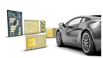
Autonomous driving and the already existing applications in this area have great potential for the microelectronics industry. The printed circuit board market for these applications is growing by roughly 5.5% annually; by 2020, the electronic components are expected to account for a share of 35% of the cost of cars, and even 50% by 2030 (Source: Statista 2018). With printed circuit boards for driver assistance systems such as distance measurement, lane change assistance and navigation systems, AT&S has already positioned itself as a technology leader at an early stage in the past.
Now AT&S is expanding its technology competence with an investment project of roughly EUR 40 million and will produce high-frequency printed circuit boards for applications which are used, for example, in sensors for distance measurements at the existing sites in Nanjangud, India (near Bangalore) and Fehring, Austria (South East Styria) starting in May 2018 (India) and March 2019 (Fehring). Both plants will continue to expand the relevant competences in close coordination and in synergy.
The new capacities will contribute to increases in revenue and earnings in the Automotive segment, which currently accounts for 33% of the Group’s total revenue together with the Industrial and Medical segments. CEO Andreas Gerstenmayer said: “We were one of the pioneers in HDI technology in the automotive sector and with this expansion we intend to consolidate our position in the future. This step is fully in line with our strategy to generate growth through technology. This is a significant technology leap for both sites. As a result, we will continue to be the technology leader in India as well, far ahead of the competition. We consider India a very lucrative future market for us.”
For autonomous driving, great volumes of complex data have to be transferred securely in split seconds. These advanced applications require high-frequency printed circuit boards, which not only serve as a connection platform for the electronic components, but also exercise the functions of antennas and filters, for example. AT&S is globally leading in this area and has developed printed circuit boards which deliver the necessary performance in the frequency range up to 80 GHz. These technologies provide the basis for powerful radar components (long-range radar with 77/79 GHz) in driver assistance systems and are thus an indispensable prerequisite for autonomous driving.
Share on:


Suggested Items
Samsung Electronics Begins Industry’s First Mass Production of 9th-Gen V-NAND
04/29/2024 | Samsung ElectronicsSamsung Electronics, the world leader in advanced memory technology, today announced that it has begun mass production for its one-terabit (Tb) triple-level cell (TLC) 9th-generation vertical NAND (V-NAND), solidifying its leadership in the NAND flash market.
TSMC Celebrates 30th North America Technology Symposium
04/29/2024 | TSMCTSMC unveiled its newest semiconductor process, advanced packaging, and 3D IC technologies for powering the next generation of AI innovations with silicon leadership at the Company’s 2024 North America Technology Symposium.
QinetiQ Achieves UK’s First Jet-to-Jet Teaming Between Aircraft and Autonomous Drone
04/29/2024 | QinetiQQinetiQ has successfully trialled the UK’s first Crewed-Uncrewed-Teaming demonstration between a crewed aircraft and an autonomous jet drone.
Warm Windows and Streamlined Skin Patches – IDTechEx Explores Flexible and Printed Electronics
04/26/2024 | IDTechExFlexible and printed electronics can be integrated into cars and homes to create modern aesthetics that are beneficial and easy to use. From luminous car controls to food labels that communicate the quality of food, the uses of this technology are endless and can upgrade many areas of everyday life.
iNEMI Packaging Tech Topic Series: Role of EDA in Advanced Semiconductor Packaging
04/26/2024 | iNEMIAdvanced semiconductor packaging with heterogenous integration has made on-package integration of multiple chips a crucial part of finding alternatives to transistor scaling. Historically, EDA tools for front-end and back-end design have evolved separately; however, design complexity and the increased number of die-to-die or die-to-substrate interconnections has led to the need for EDA tools that can support integration of overall design planning, implementation, and system analysis in a single cockpit.