


 Flexible Thinking: PCB Designers Still Wanted
 Connect the Dots: Five Best Practices for Designing Flex and Rigid-flex PCBs
 Tim’s Takeaways: Human Ingenuity and the Rigid-flex PCB
AT&S Fehring Plant: EUR 10 Million Investment and 70 New Jobs
February 12, 2018 | AT&SEstimated reading time: 1 minute
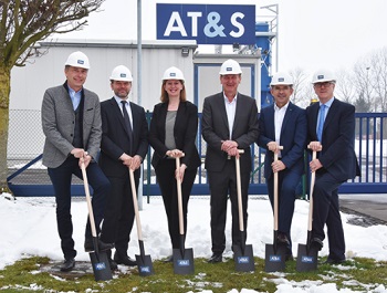
With the expansion project, which involves investments of EUR 10 million, the AT&S plant in Fehring will receive a significant technological upgrade: Starting in March 2019, high-end printed circuit boards will be manufactured in Fehring, primarily for the Automotive sector – high-frequency printed circuit boards for applications in the area of autonomous driving, for example sensors for distance measurements. In addition, products for civil aviation will be produced in cooperation with the Leoben site, as well as printed circuit boards for medical applications.
“With this technology expansion and an additional 1,200 square meters of space, around 70 new jobs will be created,” said AT&S CEO Andreas Gerstenmayer. “And the site will be secured within the AT&S Group in the long term. This is a strong signal for the industrial development in the region of South East Styria and is fully in line with our strategy to develop sites further through technology expansion. We also receive valuable support from the province of Styria in this project.”
Barbara Eibinger-Miedl, member of the provincial government responsible for economic affairs, added, “AT&S is an important lead company in Styria and makes a significant contribution to the positive development of the local economy with its research projects and products. The expansion of the Fehring site is an investment in the future, which provides for value creation, new jobs and consequently quality of life in the region. I would like to thank Andreas Gerstenmayer and the entire AT&S team for this strong commitment to Styria as a business location!”
Heinz Moitzi, chief operations officer, emphasizes the importance of the topic of qualification.
“The state-of-the-art technology used is an excellent opportunity for the employees to further improve their qualifications. This refers especially to the topic of automation and therefore represents a very good opportunity for the applications in the latest standards for Industry 4.0.”
Share on:


Suggested Items
Samsung Electronics Begins Industry’s First Mass Production of 9th-Gen V-NAND
04/29/2024 | Samsung ElectronicsSamsung Electronics, the world leader in advanced memory technology, today announced that it has begun mass production for its one-terabit (Tb) triple-level cell (TLC) 9th-generation vertical NAND (V-NAND), solidifying its leadership in the NAND flash market.
TSMC Celebrates 30th North America Technology Symposium
04/29/2024 | TSMCTSMC unveiled its newest semiconductor process, advanced packaging, and 3D IC technologies for powering the next generation of AI innovations with silicon leadership at the Company’s 2024 North America Technology Symposium.
QinetiQ Achieves UK’s First Jet-to-Jet Teaming Between Aircraft and Autonomous Drone
04/29/2024 | QinetiQQinetiQ has successfully trialled the UK’s first Crewed-Uncrewed-Teaming demonstration between a crewed aircraft and an autonomous jet drone.
Warm Windows and Streamlined Skin Patches – IDTechEx Explores Flexible and Printed Electronics
04/26/2024 | IDTechExFlexible and printed electronics can be integrated into cars and homes to create modern aesthetics that are beneficial and easy to use. From luminous car controls to food labels that communicate the quality of food, the uses of this technology are endless and can upgrade many areas of everyday life.
iNEMI Packaging Tech Topic Series: Role of EDA in Advanced Semiconductor Packaging
04/26/2024 | iNEMIAdvanced semiconductor packaging with heterogenous integration has made on-package integration of multiple chips a crucial part of finding alternatives to transistor scaling. Historically, EDA tools for front-end and back-end design have evolved separately; however, design complexity and the increased number of die-to-die or die-to-substrate interconnections has led to the need for EDA tools that can support integration of overall design planning, implementation, and system analysis in a single cockpit.