


 Flexible Thinking: PCB Designers Still Wanted
 Connect the Dots: Five Best Practices for Designing Flex and Rigid-flex PCBs
 Tim’s Takeaways: Human Ingenuity and the Rigid-flex PCB
MFS Technology Opens Fourth Manufacturing Plant
June 8, 2020 | MFS TechnologyEstimated reading time: 1 minute
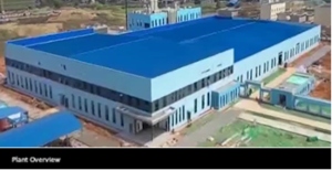
MFS Technology recently opened its fourth manufacturing plant. The new factory, which specializes in high-precision flexible printed circuit boards and electronics components assembly, is in Yiyang city’s Economic Development Zone, Hunan, China.
The first part of the two-phase development is fully completed and begins volume production in June 2020.
The new setup, which sits on 11 hectares of land, adds 300,000 sqm of capacity of MFS Technology each year.
It is equipped with the latest technology, ranging from roll-to-roll FPC (double-sided) process, class-1000 clean room and highly automated equipment. The new facility combines a high degree of machine integration with over three decades of experience accumulated in three existing factories— one in Malaysia and two in China.
A diversified pool of experienced technical and management expertise in Singapore, Malaysia and China across the organization has aided the factory’s quick and steady volume ramp-up.
Headquartered in Singapore, MFS Technology serves more than 200 multinational companies in a wide range of markets including Automotive, Industrial, Medical, Mobile, Consumer and Power Management.
“The state-of-the-art Yiyang factory adds strength to our worldwide sales to meet high volume requirement in addition to our proven capability to fulfil high mix and mid volume business,” the company mentions in a local news coverage of the new plant.
Share on:


Suggested Items
Warm Windows and Streamlined Skin Patches – IDTechEx Explores Flexible and Printed Electronics
04/26/2024 | IDTechExFlexible and printed electronics can be integrated into cars and homes to create modern aesthetics that are beneficial and easy to use. From luminous car controls to food labels that communicate the quality of food, the uses of this technology are endless and can upgrade many areas of everyday life.
iNEMI Packaging Tech Topic Series: Role of EDA in Advanced Semiconductor Packaging
04/26/2024 | iNEMIAdvanced semiconductor packaging with heterogenous integration has made on-package integration of multiple chips a crucial part of finding alternatives to transistor scaling. Historically, EDA tools for front-end and back-end design have evolved separately; however, design complexity and the increased number of die-to-die or die-to-substrate interconnections has led to the need for EDA tools that can support integration of overall design planning, implementation, and system analysis in a single cockpit.
Koh Young Showcases Award-winning Inspection Solutions at SMTconnect with SmartRep in Hall 4A.225
04/25/2024 | Koh Young TechnologyKoh Young Technology, the industry leader in True 3D measurement-based inspection solutions, will showcase an array of award-winning inspection and measurement solutions at SMTconnect alongside its sales partner, SmartRep, in booth 4A.225 at NürnbergMesse from June 11-13, 2023. The following offers a glimpse into what Koh Young will present at the tradeshow:
Real Time with… IPC APEX EXPO 2024: Plasmatreat: Innovative Surface Preparation Solutions
04/25/2024 | Real Time with...IPC APEX EXPOIn this interview, Editor Nolan Johnson speaks with Hardev Grewal, CEO and president of Plasmatreat, a developer of atmospheric plasma solutions. Plasmatreat uses clean compressed air and electricity to create plasma, offering environmentally friendly methods for surface preparation. Their technology measures plasma density for process optimization and can remove organic micro-contamination. Nolan and Hardev also discuss REDOX-Tool, a new technology for removing metal oxides.
Nanotechnology Market to Surpass $53.51 Billion by 2031
04/25/2024 | PRNewswireSkyQuest projects that the nanotechnology market will attain a value of USD 53.51 billion by 2031, with a CAGR of 36.4% over the forecast period (2024-2031).