


 Flexible Thinking: PCB Designers Still Wanted
 Connect the Dots: Five Best Practices for Designing Flex and Rigid-flex PCBs
 Tim’s Takeaways: Human Ingenuity and the Rigid-flex PCB
Catching Up (Literally) with Uyemura’s George Milad at SMTAI 2016
November 14, 2016 | Patty Goldman, I-Connect007Estimated reading time: 12 minutes
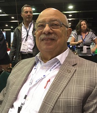
I managed to catch up with George Milad of Uyemura at the recent SMTA International conference, which wasn’t easy to do. But he did take a few minutes to fill me in on his schedule for the week and it certainly was packed, with a tutorial, presentations and IPC committee meetings.
Patty Goldman: Hi, George, it’s great to see you again—about twice a year, right? Let’s talk a little bit about what you’re presenting here at the SMTAI conference.
George Milad: I have had a very busy schedule. Yesterday I gave a presentation, a four-hour tutorial, and I will never do that again. To stand up and talk for four complete hours, it's very challenging staying alert and relevant and keeping the audience’s attention and making sure you're delivering value, because these people paid money to sit in that meeting. That was very challenging but it went very well and I'm happy. I get energized by the feedback from the attendees in the class, but then when I got back to my hotel, I was trying to listen to the presidential debate and I fell asleep after the first five minutes. (Laughs)
Goldman: I heard it was not that exciting of a debate, anyhow. But that does sound exhausting. How many people were in your audience?
Milad: We had approximately 15 people who signed up and paid money. That is very rewarding, because I gave the same training course at PCB West and I think if you signed up it was free, and I had three people show up. I talked forever for three people and it kills your energy, but this one was a very rewarding experience.
Goldman: You imparted a lot of knowledge.
Milad: Yes, they thought it was good. They filled in the forms and so I'll get some feedback from SMTA. Then first thing in the morning tomorrow I'm going to talk about the “Via Fill Copper Plating Process” and what it takes to optimize the via fill process. I-Connect007 published an article along these lines recently and this is basically the same concept but in the form of a presentation rather than an article.
Then I have the IPC 4-14 Plating Processes subcommittee meeting. Our committee meetings are not so critical because we do our work by conference call.
Goldman: Yes, I was very impressed when we talked about that before. I've been very impressed with how you guys conduct those meetings every…how many weeks?
Milad: Every other week.
Goldman: You get a lot accomplished that way.
Milad: Indeed. Then you set things in motion, and you say, "Okay, we need to just make a test vehicle (TV) ." Somebody manufactures it and then every couple of weeks we find out the status, and when the TV is complete, we send it out to people to plate it. Then we send it back out for evaluation We're always following these activities and evaluating results, and then we begin to write the specification and get interaction from people who sometimes like what's being written or some people take a strong objection to what's being written. And for good reason—I'm not saying they will just object for the sake of objecting.
For this, we were rewriting the ENIG spec. We wanted to set the upper limit for ENIG. It was written in 2002.
Goldman: That's a long time ago.
Milad: Yeah, 14 years later we're revising the specification. In 2002, we agreed that gold should be a minimum of two microinches. We did not put an upper limit, but we wrote that it should typically be 3−5 microinches. Typically, 3−5 is not the specification. Minimum of 2 microinches is the specification. Anybody who read the specification said the IPC calls for 3−5 μins, which was a horrible thing. We never called for 3−5 μins and it created a lot of problems.
Now, we’ve come back and we are redefining the gold thickness. We put the lower limit of 1.6 μins instead of two. Then, we wanted to put an upper limit. We tried very hard to pass 3.2 μins as the upper limit. We got a lot of resistance from manufacturers who do ENIG surface finish for the medical industry. They called for a minimum of 3.0 μins. They are the biggest printed circuit shop in the United States, I don't feel I should mention their name, but they said they have medical customers who will require a 3.0 μins minimum. We wanted to put 3.2 as the maximum, leaving no room at all to work between 3.0 and 3.2 μins. They kept arguing and finally we conceded and we put 4.0 μins as the upper limit. That is what the new specs will say, 1.6 to 4.0 μins. This is the first time we put an upper limit and as far as the 3−5 μins, we're hoping that will go by the wayside.
Goldman: I imagine it is a problem to put too much down, isn't it?
Milad: Absolutely. The problem with putting too much down is you're staying in the gold bath for a prolonged amount of time and that gives a lot of opportunity for nickel corrosion, or black pad. It's always been our objective to say, “Don't do that. You need only 2.0 μins. Get them deposited on the nickel and get out of the bath. There is no reason to stay any longer.”
It's not that it's guaranteed that if you stay longer in the bath that you're going to have corrosion, but if the nickel is a little bit compromised, it's not the perfect nickel, and you stay too long you will get corrosion. If you have the perfect nickel, it can withstand prolonged dwell in the gold bath, but nobody makes perfect nickel 100% of the time. We felt it's very important to restrict the gold thickness.
Goldman: This corrosion you're talking about is black pad, right?
Milad: Yes, the nickel corrosion and black pad are synonymous. If it is too extensive, then the pad is not going to solder, and the whole objective of the ENIG finish is that it’s a solderable finish. That's the story there. We don't want you to stay too long in the gold baths.
We also are including a corrosion chart in this new revision of the ENIG specification, which was quite challenging because when you have corrosion and you do a cross-section, it appears as spikes. When you look at a cross-section under 1000x magnification and you see less than 10 spikes in the field of view, that's acceptable. If you have more than 10 spikes, that's not acceptable. If the spikes are joined together, meaning they blend, one spike runs into the other, that's not acceptable. If the spike is too deep, that's not acceptable. We specified that and we ran into a huge tizzy of argumentation.
Is it 10? Is it 8? Is it 9? Is it 11? Is it 12? We finally said that we're just going to define what is acceptable and we're going to define what is rejectable. We're going to admit that there is a gray area between acceptable and rejectable.
Goldman: Yes, like saying 10 is good but 11 is bad? It seems that people might say, "Wait a minute. That's not that bad, is it?”
Milad: Yeah, so we decided to leave everything in between for the buyer and the manufacturer to sort out. If it's less than 10, we don't want any argument. We want this to be acceptable.
Page 1 of 2
Share on:


Suggested Items
Connect the Dots: Designing for Reality—The Pre-Manufacturing Process
05/08/2024 | Matt Stevenson -- Column: Connect the DotsI have been working with Nolan Johnson on a podcast series about designing PCBs for the reality of manufacturing. By sharing lessons learned over a long career in the PCB industry, we hope to shorten learning curves and help designers produce better boards with less hassle and rework. Episode 2 deals with the electronic pre-manufacturing process. Moving from CAD (computer-aided design) to CAM (computer-aided manufacturing) is a key step in PCB manufacturing. CAM turns digital designs into instructions that machines can use to actually build the PCB.
AIM Solder Signs Shinil Fl Ltd. as New Distributor for Korea
05/08/2024 | AIM SolderAIM Solder, a leading global manufacturer of solder assembly materials for the electronics industry, is pleased to announce a new distribution partnership with Shinil Fl Ltd., a prominent supplier of technological solutions in the SMT and semiconductor sectors.
Indium Corporation to Showcase HIA Materials at ECTC
05/07/2024 | Indium CorporationAs an industry leader in innovative materials solutions for semiconductor packaging and assembly, Indium Corporation® will feature its advanced products designed to meet the evolving challenges of heterogeneous integration and assembly (HIA) and fine-pitch system-in-package (SiP) applications at the 74th Electronic Components and Technology Conference (ECTC), May 28‒31, in Denver, Colorado.
Indium Corporation Expert to Present on Pb-Free Solder for Die-Attach in Discrete Power Applications
04/30/2024 | Indium CorporationIndium Corporation Product Manager – Semiconductor Dean Payne will present at the Advanced Packaging for Power Electronics conference, hosted by IMAPS, held May 8-9 in Woburn, Massachusetts, USA.
Taiyo Circuit Automation Installs New DP3500 into Fuba Printed Circuits, Tunisia
04/25/2024 | Taiyo Circuit AutomationTaiyo Circuit Automation is proud to be partnered with Fuba Printed Circuits, Tunisia part of the OneTech Group of companies, a leading printed circuit board manufacturer based out of Bizerte, Tunisia, on their first installation of Taiyo Circuit Automation DP3500 coater.