


 The Chemical Connection: Reducing Etch System Water Usage, Part 2
 It’s Only Common Sense: Nice Guys Really Can Finish First
 The Right Approach: I Hear the Train A Comin'
Japan Flexes Its Advantages in Semiconductor Upstream Equipment and Raw Materials
October 31, 2023 | TrendForceEstimated reading time: 3 minutes
In the face of unceasing geopolitical upheavals in recent years, nations worldwide are striving to cultivate homegrown semiconductor supply chains and fortify the stability of their industrial supply dynamics. At present, Taiwan stands tall as a global powerhouse when it comes to semiconductor foundries. TrendForce data showcases that as of 2Q23, Taiwanese firms collectively command a hefty 65% market share in global foundry revenue, with TSMC alone claiming a whopping 56%. This underscores Taiwan’s crucial position globally and has motivated regions worldwide to establish semiconductor industries within their territories while considering a multitude of factors.
Beyond attracting leading tech giants to establish manufacturing bases, venturing into self-driven R&D has emerged as a viable alternative.
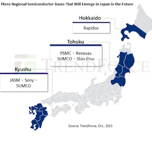
TrendForce points out that Japan is also attempting to seize this opportunity for reshuffling, aiming to reclaim the 40 years lost in its semiconductor industry. Based on Japan’s geographical characteristics, TrendForce has identified three potential semiconductor hubs that might emerge in Japan, located in Kyushu, Tohoku, and Hokkaido respectively.
I. Kyushu
Kyushu has swiftly ascended as a semiconductor hotspot, thanks in part to the advent of JASM (TSMC’s Kumamoto Plant). Even prior to TSMC’s entry, Sony and SUMCO, a behemoth in raw wafer production, have been operating in the region for several years. Additionally, numerous small and medium-sized semiconductor-related enterprises have established themselves in the region, rightfully earning Kyushu the title of "Silicon Island."
With JASM slated for completion, it is set to house one of the most advanced semiconductor factories in the region, embracing manufacturing processes ranging from 12 to 28nm. Even a future migration to more advanced processes is on the table depending on customer demand.
Given its strategic location adjacent to Sony’s existing CIS factory, and considering Sony’s stake in JASM, expect a synergy that strengthens their collaboration in semiconductor manufacturing and packaging and testing technologies.
II. Tohoku
If Japan is considered a global hub for the production of semiconductor raw materials, then the Tohoku region serves as the heart of this crucial industry. This region, enveloping areas around Sendai and Fukushima, is home to the Renesas Yonezawa plant, and major raw wafer producers SUMCO and Shin-Etsu. Bolstered by Tohoku University’s reputation in semiconductor materials research and a rich talent pool, Tohoku stands out.
On October 31st, PSMC officially unveiled plans to build a 12-inch wafer plant in Sendai, initially focusing on the 40nm process node, with advanced processes in the roadmap. Automotive electronics will be a production priority, further amplifying Tohoku’s semiconductor significance.
III. Hokkaido
Rapidus, a Japanese enterprise aiming high with 2nm semiconductor technology, has surprisingly chosen Hokkaido as its base, catapulting the region into Japan’s third semiconductor stronghold. Government plans indicate that Rapidus could be a magnet for upstream equipment and material suppliers to flock to Hokkaido, potentially sparking a semiconductor community boom. Its proximity to Chitose Airport also promises seamless talent and resource flow. With the factory under construction and set to complete in 2024, and mass production earmarked for 2027, Rapidus is on track, with much of its R&D conducted in collaboration with IBM in the United States, showcasing Japan’s ambition to spearhead advanced semiconductor manufacturing.
Japan’s resurgence in the semiconductor arena is palpable, with the Ministry of Economy, Trade, and Industry fostering multi-faceted collaborations with the private sector. With a favorable exchange rate policy aiding factory construction and investments, the future looks bright for exports. However, the looming shortage of semiconductor talent in Japan is a concern. In response, there are generous subsidy programs for talent development. Japan is strategically positioning itself to reclaim its former glory in the world of semiconductors.
Share on:


Suggested Items
ZESTRON Academy Launches 2024 Advanced Packaging & Power Electronics Webinar Series
05/01/2024 | ZESTRONZESTRON, the leading global provider of high-precision cleaning products, services, and training solutions in the electronics manufacturing and semiconductor industries, proudly announces the launch of its highly anticipated webinar series on Advanced Packaging & Power Electronics, a webinar series on the latest innovations, cleaning, and corrosion challenges.
Worldwide Silicon Wafer Shipments Dip 5% in Q1 2024
05/01/2024 | SEMIWorldwide silicon wafer shipments decreased 5.4% quarter-over-quarter to 2,834 million square inches in the first quarter of 2024, a 13.2% drop from the 3,265 million square inches recorded during the same quarter last year, the SEMI Silicon Manufacturers Group (SMG) reported in its quarterly analysis of the silicon wafer industry.
Guerrilla RF Completes Strategic Acquisition of GaN Device Portfolio from Gallium Semiconductor
04/29/2024 | BUSINESS WIREGuerrilla RF, Inc. has finalized the acquisition of Gallium Semiconductor's entire portfolio of GaN power amplifiers and front-end modules. Effective April 26th, 2024, GUER acquired all previously released components as well as new cores under development at Gallium Semiconductor.
SIA Commends CHIPS Act Incentives for Micron’s Manufacturing Projects in New York and Idaho
04/29/2024 | SIAThe Semiconductor Industry Association (SIA) today released the following statement from SIA President and CEO John Neuffer applauding semiconductor manufacturing incentives announced by the U.S. Department of Commerce and Micron.
iNEMI Packaging Tech Topic Series: Role of EDA in Advanced Semiconductor Packaging
04/26/2024 | iNEMIAdvanced semiconductor packaging with heterogenous integration has made on-package integration of multiple chips a crucial part of finding alternatives to transistor scaling. Historically, EDA tools for front-end and back-end design have evolved separately; however, design complexity and the increased number of die-to-die or die-to-substrate interconnections has led to the need for EDA tools that can support integration of overall design planning, implementation, and system analysis in a single cockpit.